Molecular Beam Epitaxy (MBE) is an ultra-high vacuum (UHV) thin film deposition technique that is widely regarded as the most controlled and highest purity form of deposition, used in both research and mass production.
MBE involves keeping a crystal substrate at a certain growth temperature in an ultra-high vacuum environment. The elements that make up the growing material are placed in separate source cells. By controlling the temperature of the source cells, a quantitatively controlled molecular beam is achieved through thermal evaporation, which is directed towards the crystal substrate. The ultra-high vacuum ensures that the particles within each beam do not collide with each other. The various molecular atoms reaching the crystal surface undergo a series of processes such as surface adsorption, dissociation, surface migration, and bonding to form an epitaxial layer crystal. It is a complex dynamical physical process. By independently controlling the temperature of each source cell, as well as the shutter switches and timing, it is possible to achieve heteroepitaxial growth, different material thickness, alloy composition, and doping concentration on different materials.
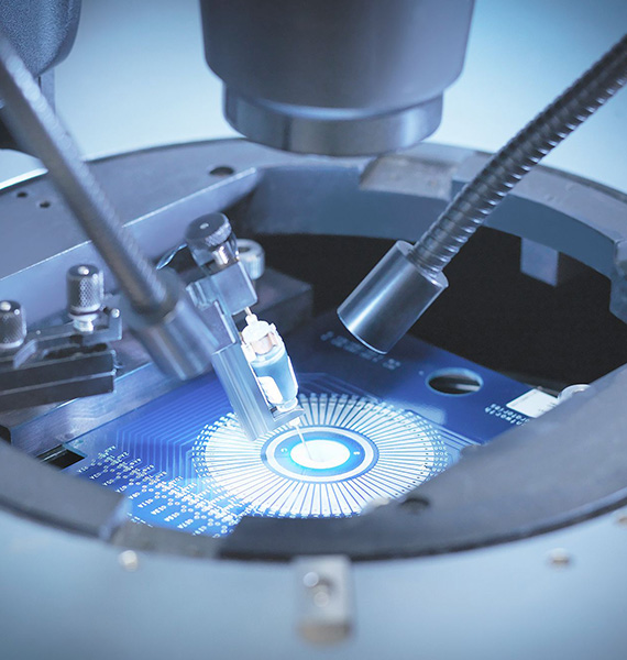
MBE equipment typically consists of a growth chamber, a pre-processing chamber, and a load-lock chamber, with the growth chamber being the core component. The load-lock chamber is used for loading and unloading substrates and epitaxial materials, while the pre-processing chamber is used for surface treatment of the substrates before epitaxial growth and temporary storage of samples. The growth chamber primarily consists of a vacuum system, a control system, and an in-situ monitoring system. By optimizing the design and using cryogenic pumps and ion pumps, the growth chamber can achieve ultra-high vacuum conditions. Liquid nitrogen shields are cleverly placed around the high-temperature components of the sample holder and the source furnaces, ensuring isolation between the source cells and efficient adsorption of atoms and molecules reaching the chamber walls. This effectively maintains an ultra-high vacuum, enabling the growth of semiconductor heterostructures with extremely low background impurities and high electron mobility.
The control system consists of mechanical and electrical controls for sample transfer, sample holder rotation, source shutter operation, and source cell temperature. It includes various power supplies, controllers, pressure and temperature sensors, as well as software for epitaxial growth controls and equipment safety controls.
The most commonly used in-situ monitoring tool in MBE is Reflection High-Energy Electron Diffraction (RHEED). RHEED utilizes a high-energy electron beam (typically >=15 keV) to impinge on the substrate at a nearly vertical angle (usually 2°), causing it to diffract with the surface layer and form a diffraction pattern on a phosphor screen. By analyzing the diffraction pattern, rich information about the surface can be obtained, including crystal structure, atomic spacing, surface quality, and growth rate, which cannot be achieved by other epitaxial techniques.
MBE is widely employed in the research and production of materials and devices for semiconductor high-speed microelectronics, optoelectronics, and quantum information fields. It is an indispensable industrial fabrication technology for high-end information functional materials.