
ABOUT ATOMAN
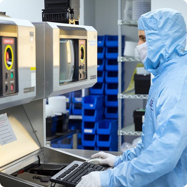
With the philosophy of building an epitaxial ecosystem, Atoman continues to carry out scientific and technological innovation, and provides customers with epitaxy material solutions through its own research and development team. Since establishment, we have established epitaxial factories in multiple locations, including Beijing, Xiamen, Zhuji, and Finland. Our products are widely used in various fields such as 5G communication, data centers, electric vehicles, MicroLED, photovoltaics, and more.
EPIWAFER

|
GaAs GaAs epitaxial materials demonstrate excellent performance in the fields of radio frequency (RF) and optoelectronics. GaAs pHEMT is widely used in wireless communication RF front-end modules, while GaAs VCSEL is extensively applied in 3D sensing and data centers. To meet the performance requirements of RF and optoelectronic chips, Atoman utilizes internationally leading MBE epitaxial production technology, offering high-quality GaAs epitaxial wafers to customers worldwide. |

|
InP InP epitaxial materials are widely used in the near-infrared detection, optical communication, and high-frequency microwave RF fields due to their excellent performance in the near-infrared wavelength range and ultra-high electron mobility. With the increasing demand for data transmission efficiency in modern technology, high-speed optical communication requires chips with continuously improving performance. To meet the performance requirements of optoelectronic and RF chips, Atoman utilizes internationally leading MBE epitaxial production technology, providing high-quality InP epitaxial wafers to customers worldwide." |

|
GaN GaN is a representative of third-generation semiconductor materials, known for its advantages such as high breakdown voltage and high saturation rate. It is gradually replacing traditional silicon-based devices and plays a significant role in the fields of microwave RF and power electronics. Atoman utilizes internationally leading Hybrid-MBE technology to provide high-quality and cost-effective GaN epi-wafers to customers both domestically and internationally. |


TECHNICAL SERVICE
We provide MBE equipment repair, mechanical structure maintenance, chamber cleaning, equipment relocation, and technical consulting services for our customers.

PRODUCTION LINE COOPERATION
We offer guidance on the construction of epitaxial production lines, plant management, and analysis of plant operations to assist our customers in effectively utilizing equipment for research and production purposes.
NEWS&MEDIA


JOIN US
Atoman Semiconductor is committed to discovering and cultivating young talents and top experts in the MBE field. We sincerely invite individuals with a passion for advancing in the MBE industry, possessing innovative thinking, daring to dream big, and full of enthusiasm to join us!
